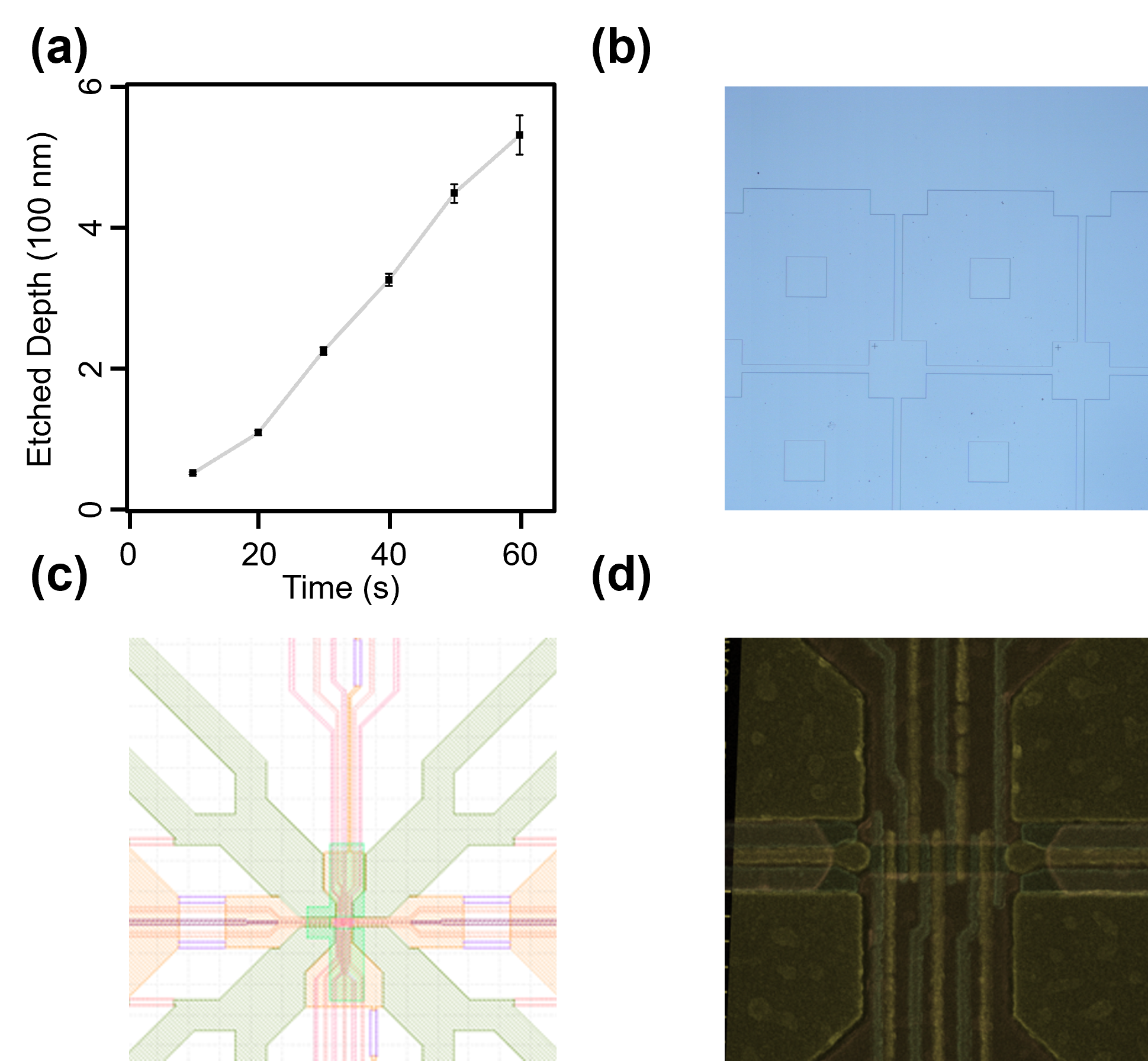
Figure 1 Key Steps in the Nanofabrication of a Silicon Quantum Dot Device. (a) Calibration of the reactive ion etching (RIE) rate for the Si/SiGe substrate. The etching was performed using $\mathrm{SF_6/O_2}$ plasma at 30 W RF power, yielding a linear etch rate of approximately 10.9 nm/s. (b) Optical microscope image of the device mesa structure after the RIE process. The calibrated etch rate from (a) was used to precisely control the etch depth to define the active device area. (c) Computer-aided design (CAD) layout of the multi-layered, overlapping nanogates. This complex pattern is designed for high-resolution electron-beam (E-beam) lithography. (d) Scanning electron microscope (SEM) image of the final device after E-beam lithography, Ti/Pd metal deposition, and liftoff.
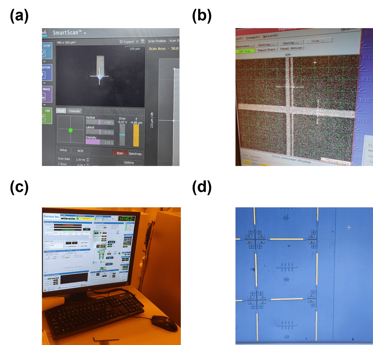
Figure 2 Key Fabrication and Characterization Tool Interfaces and Processes. (a) In-situ laser alignment of a cantilever for an Atomic Force Microscope (AFM), a critical calibration step required for the precise topographical characterization of nanoscale device features. (b) Locating a global alignment marker using the backscattered electron (BE) signal in an electron-beam (E-beam) lithography system. This is an essential process for establishing a coordinate system for high-precision, multi-layer patterning. (c) The user interface of a thin-film deposition system during the adjustment of a process recipe (e.g., for Atomic Layer Deposition or E-beam evaporation), which allows for precise control over deposition parameters. (d) An optical microscope image of large-scale gold alignment markers patterned on the chip. These markers are used for global alignment in subsequent photolithography and E-beam lithography steps.
Device Fabrication Mar. 2023 – Dec. 2024
⌜Led the end-to-end cleanroom fabrication of multi-layered silicon quantum dot devices. Utilized a hybrid lithography approach, combining maskless photolithography for large features and E-beam lithography for nanoscale gates. Developed a process for overlaid gate structures requiring high-precision alignment to prevent spurious quantum dots, and implemented manual E-beam focus correction to overcome pattern blurring from large marker topography. The full process involved RIE/wet etching, ALD for dielectric layers, and rigorous AFM/SEM metrology.⌟
In a semiconductor quantum dot device, the precise manipulation of individual electrons is achieved
by applying voltages to metallic nanogates, forming potential landscapes that confine particles and define
the energy levels of a qubit. To meet the exacting nanometer-scale dimensions required, the utilization of
electron-beam (E-beam) lithography becomes imperative for patterning these critical features.
My work involved the complete, end-to-end fabrication of multi-layered silicon quantum dot devices,
starting from a bare Si/SiGe quantum well wafer. The process began with defining the active device area via
mesa etching, where I gained experience with both dry (Reactive Ion Etching) and wet (chemical)
etching techniques. This was followed by defining ohmic contacts through phosphorus ion implantation and
rapid thermal annealing (RTA).
A critical challenge in silicon is preventing the formation of spurious quantum dots between gates. To address this, we employed an overlaid gate structure, which demands exceptional alignment between multiple layers. To achieve this, I implemented a comprehensive alignment strategy using a full set of P, Q, R, and S markers for maximum precision.
The core of the fabrication relied on a hybrid lithography approach:
I used a maskless photolithography system for large-scale patterns like pads and markers,
and an E-beam lithography system for the fine, nanometer-scale gates.
A practical challenge I solved during E-beam writing was the blurring of patterns due to the significant
topography of the pre-etched alignment markers (2-3 µm deep).
To overcome this, I developed a protocol involving manual focus and stigmation adjustments for each marker,
ensuring sharp and accurately placed nanogates.
The multi-layered gate stack was built up through successive steps of E-beam lithography,
metal deposition via E-beam evaporation, and liftoff,
with each gate layer isolated by a thin film of Al₂O₃ deposited via Atomic Layer Deposition (ALD).
Intermediate cleaning steps, such as using O₂ plasma ashing to remove photoresist residue,
were employed to maintain device quality.
Throughout the entire process, rigorous characterization and calibration were performed using tools such as
Atomic Force Microscopes (AFM) and Scanning Electron Microscopes (SEM) to verify critical dimensions,
etch depths, and alignment accuracy. This systematic and detail-oriented approach to fabrication was essential
for producing the high-quality, reliable quantum devices used in my subsequent measurement experiments.